AI Generated Image
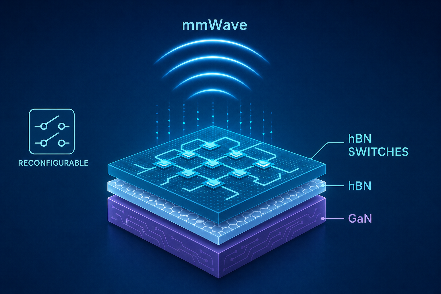
Reconfigurable mmWave microchips co-integrating hBN switches on GaN
Nature • • technology
Key Points:
- Au/hBN/Au switches exhibit ohmic conduction in the low resistance state (LRS) with forming voltages following a power-law relationship, and LRS resistance shows no clear dependence on the sweep rate during forming.
- Device cycling tests at room temperature and 175 °C reveal no significant differences in set voltages across different forming and testing conditions, with variability in high resistance state (HRS) mainly due to reset process fluctuations.
- Thermal scanning probe microscopy (SThM) experiments indicate that hBN has a larger lateral thermal conductivity than HfO2, resulting in a wider thermal profile in Au/hBN/Au devices under current flow.
- S-parameter measurements from multiple chips and hBN suppliers demonstrate consistent RF performance up to 50 GHz, with variability within expected limits and confirmed by BEOL-fabricated references.
- Power linearity tests show that shunt devices have better linearity and higher 1 dB compression points (P1dB) than series devices, consistent with their complementary conductive states and asymmetric set/reset voltages affecting power handling.


