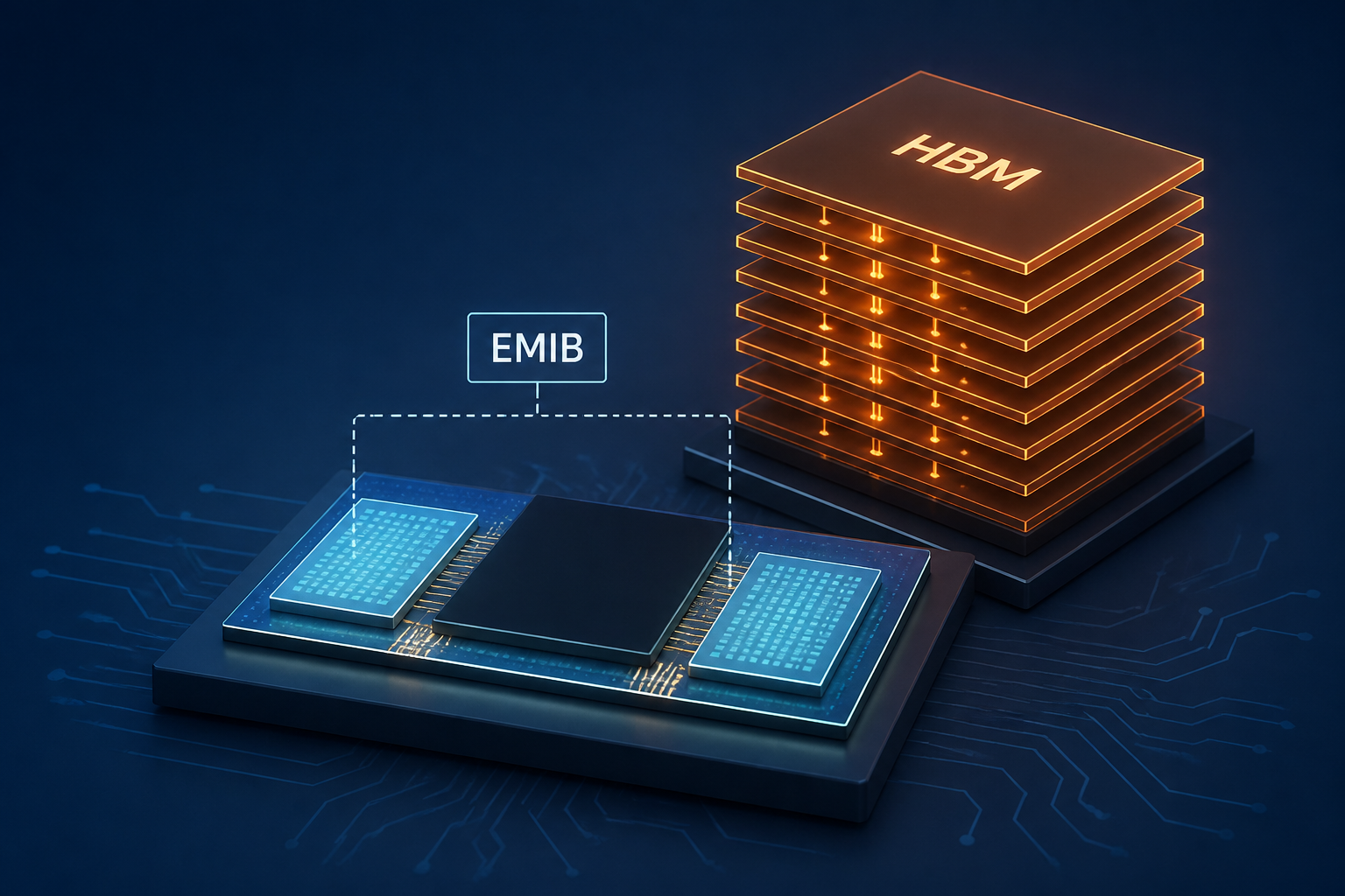
AI Generated Image
SK Hynix Unpacks Advanced Packaging Technologies, Including Intel EMIB, For Its Next-Gen HBM Memory As It Eyes 3D Structures For The Future
Wccftech • • technology
Key Points:
- SK Hynix is advancing its High-Bandwidth Memory (HBM) technology by leveraging advanced packaging solutions like Intel's EMIB and is preparing to enter the 3D packaging era to address scaling challenges.
- The company’s HBM4 roadmap targets up to 36 GB capacity, 2048 IO bits, 8 Gbps IO speeds, and over 2 TB/s bandwidth, with improvements in power efficiency and thermal resistance compared to HBM3E.
- SK Hynix employs two main packaging methods—TC+NCF and MR+MUF—with ongoing innovations such as warpage control, fine pitch interconnects, and narrow gap-fill to enhance performance and reliability.
- To tackle thermal and power challenges from increasing TSV counts and bandwidth demands, SK Hynix is developing hybrid bonding, which offers better thermal conductivity, narrower pitches, and lower thermal resistance, alongside localized hotspot mitigation technology (I-HBM).
- Looking forward, SK Hynix aims to integrate logic processes for higher IO speeds, increase TSV density, and pursue 3D stacking of HBM on accelerators, relying on industry collaboration and advanced packaging technologies to meet future capacity and bandwidth needs.


